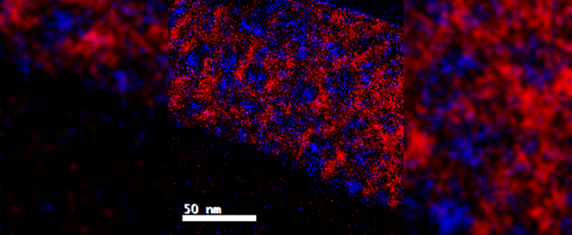
This often occurs below 100nm. The shrinkage of at least one dimension below this level results in modification of the physical, chemical and biological properties in unexpected ways. These exciting properties are the focus of the emerging field of nanoscience, and nanotechnology.
The heart of nanoscience and nanotechnology is the ability to form nanomaterials in a controlled way. The microelectronic industry utilizes “top down” miniaturization techniques (e.g. lithography) in which nanostructures are “carved” into bulk materials. In contrast, current efforts employ “bottom up” techniques which structure the material from the atomic and molecular level. Controlled nano-structuring is the focus of several groups in the Department of Materials Engineering. The structure and properties of these materials are studied, and some groups also apply nanomaterials for a variety of applications.


