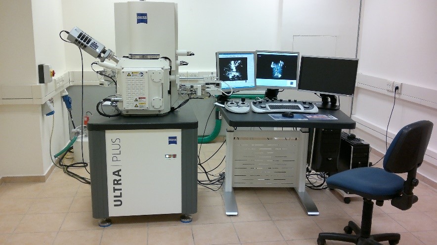
The High-Resolution Scanning Electron Microscope (HR-SEM) is used for direct imaging of surface morphology, surface fracture, thin layers, chemical composition (using EDS – Energy Dispersive Spectroscopy), crystallographic structure determination) using TKD – Transmission Kikuchi Diffraction and EBSD – Electron Back Scattered Diffraction( in various modes of scanning. The device is equipped with a FEG (Field Emission Gun) electron source, an innovative lens system and advanced sensors. The combination makes possible to obtain a spatial resolution of a few nanometers, optimizing work conditions that allow high-resolution imaging of non-conductive and semiconductor materials without the need for conductive coating.
In addition, the microscope is equipped with a STEM (Scanning Transmission EM) detector that allows the characterization of thin samples.
Using the HR-SEM, one can perform special experiments, such as heating up to 1050°C and nano-indentation experiments to test mechanical properties at the nanometer scale.