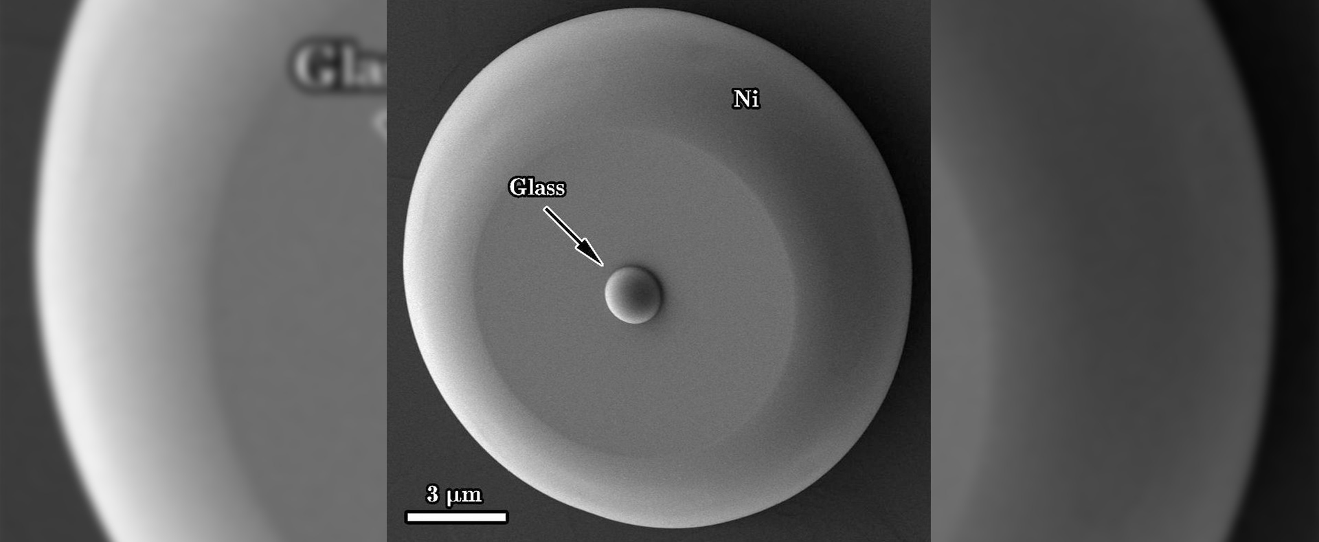
Therefore, state-of-the-art characterization techniques are utilized to study material structure and microstructure at various length scales. This plays a major role in solving important problems in the field.
The Department of Materials Science and Engineering offers world-class state-of-the-art characterization facilities which include electron microscopy (link to Mika); high-resolution scanning electron microscopy (HRSEM), a transmission electron microscope (TEM), an aberration-corrected monochromatized high-resolution Titan Themis TEM, as well as one-of-a-kind a Xe plasma focused ion beam (FIB) which is coupled with in-situ micro-Raman and Time-of-Flight Secondary Ion Mass Spectrometry (FIB-ToF-SIMS), X-ray diffraction facilities which include a multi-purpose high-resolution diffractometry system (SmartLab) and a MiniFlex. Atomic force microscopy facilities available at the Department enable observing and studying surface properties and topography at the sub nano-scale resolution.


