Prof. Eizenberg has carried out research in diverse areas of materials, including semiconductors, metal surfaces and thin films, and dielectric thin films, with the aim of correlating physical properties such as structure and composition with electrical properties. His recent research focuses on interconnects and metallization technologies (front-end and back-end) for microelectronic devices.
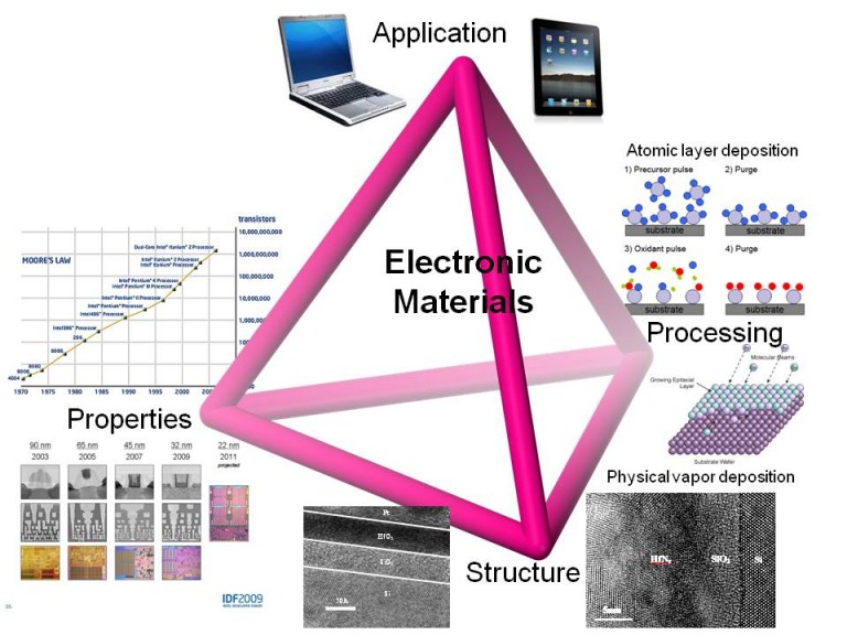
The realization of microelectronic devices with nanometric dimensions relies on the successful integration of new materials into the existing production scheme. When the thickness of SiO2, which was used as the gate dielectric in traditional MOS devices, was reduced to few nanometers due to the scaling rules imposed by Moore’s law, tunneling current became significant. The increased leakage degraded the performance of devices, by changing the turn-on voltage of FETs and decreasing the retention time of capacitors. Replacing the SiO2 with a high-k dielectric enabled using a thicker gate dielectric layer, while maintaining high capacitance values and FET channel conductance.
The required replacement of SiO2 as the gate oxide was followed by an additional process: the replacement of the traditional doped poly-Si electrode by a metallic gate. The selection of a suitable metal/ high-k stack depends both on device requirements and material properties. And finally, future scaling of devices will be achieved by using high mobility (high injection velocity) and low bandgap semiconductors as channel materials on a Si platform. The leading candidate for an n-type channel material is InGaAs, and Ge is for p-type. In parallel there is an effort to use wide bandgap semiconductors, such as GaN, for power electronics applications.
Eizenberg’s group has responded to these challenges by putting a strong emphasis on studying metal/high-k interfaces for future memory and high-performance devices. Various materials, such as Al2O3, HfO2 and lanthanide oxides (e.g. Gd2O3) as well as some nitrides were studied in his laboratory as gate dielectrics, and the interface between these dielectrics and various metals was explored. More recently these gate stacks are studied on top of other semiconductors than Si such as Ge, InGaAs, and GaN. This important research enables understanding the correlation between materials properties (e.g. interface composition, structure and binding) and electrical properties of metal/high-k/semiconductor stacks. In particular, the group has important achievements in understanding the effect of various properties on the effective work-function at the interface. Such an understanding enables to develop processes for tuning the Fermi-level position at metal/high-k interfaces.
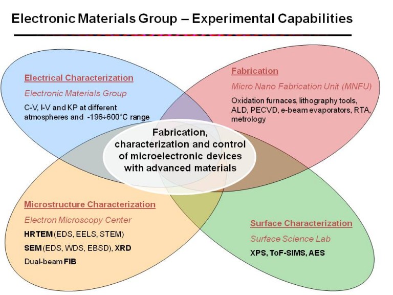
Experimental Capabilities
CURRENT RESEARCH PROJECTS
- The Role of Interfacial Composition on the Electrical Properties of Metal / High-K Dielectric / Semiconductor Interfaces.
- Tuning of Fermi Level Position at Metal / High-K Dielectric Interfaces.
- Metal and Metal-Nitride Deposition by Plasma Enhanced Atomic-Layer-Deposition (PE-ALD) for 3D devices.
- Ferroelectric HfO2-based Thin Films Deposited by PE-ALD for advanced memories.
- Advanced Schemes for Ohmic Contact Formation on SiGe.