Mr. Or Azulay - M.Sc. Candidate
13/07/2025
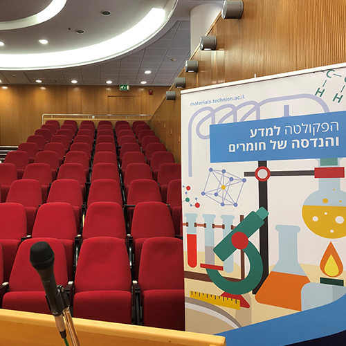
David Wang Auditorium, 3rd floor Dalia Meidan Bldg.
13:30
Gallium nitride (GaN), of the III-N family, is a wide bandgap, high electron mobility and high breakdown field semiconductor material. Moreover, due to its Wurtzite structure, it has a permanent polarization along the c-axis ([0001]) and is similarly piezoelectric. Piezoelectric materials are usually dielectric, therefore the coupling of the piezoelectric properties and the semiconducting properties in GaN opens up possibilities for new applications. Nano-porosity is a known way of controlling both optical and mechanical properties of GaN and other materials based on specific needs. Recent findings suggest that
nano-porosity could boost GaN’s electromechanical coupling, potentially enhancing its piezoelectric capabilities.
In this talk I will discuss the development of a fabrication process to create dry etched nanopores in GaN, the chosen pattern, the characterization methods and analysis of the data. Briefly, a specialized process was developed by using electron beam lithography (EBL) and dry etching with plasma in inductively
coupled plasma reactive ion etching (ICP-RIE). The piezoelectric characterization was carried out using piezo-response force microscopy (PFM). The acquired trends and phenomena will be compared with a finite element method (FEM) simulation and other models in order to obtain a sufficient explanation for piezoelectric response, considering the mechanical effects of porosity and the semiconducting nature of the material.


