

Prof. Oana Cojocaru-Mirédin
11/02/2026
אודיטוריום ע"ש דויד וואנג, בניין מידן, קומה 3
12:30
Correlative Microscopy & Techniques (CM&T), which is the combination of atom probe tomography with other (microscopy) techniques, has become a very powerful approach, which has made considerable progress in Materials Science. CM&T helps to better understand the correlation between individual material properties (chemical, structural, electrical or/and optical properties) at the same position on the sample. This type of information is crucial for the rational design of advanced materials with superior properties, and―when integrated in devices―with superior performance. Moreover, this approach opens the possibility to answer long-standing questions in material science, such as the impact of the grain boundaries' chemistry and structure on the electronic properties (see example from Figure 1).
This lecture will show a selection of several examples where APT was combined with transmission electron microscopy and electron backscatter diffraction [1] to establish chemistry-structure correlations for a large variety of materials, starting with metallic systems and ending with the ceramic ones. Moreover, examples of chemistry-structure-electronic properties correlations [2],[3] will be provided with a specific focus on defect engineering.
Finally, this lecture will demonstrate how the device performance can be manipulated by the correlations between structure and property down to the interface level, providing a novel bottom-to-top strategy for the material design.
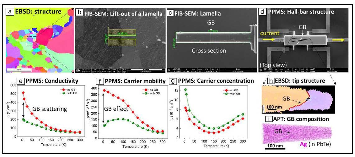
Figure 1. Example of a direct correlation between the grain boundary composition with their respective structure and transport in PbTe thermoelectrics [2]. Bibliography: [1] O. Cojocaru-Mirédin, T. Schwarz, and D. Abou-Ras, “Assessment of elemental distributions at line and planar defects in Cu (In, Ga) Se2 thin films by atom probe tomography,” Scr. Mater. 148 106 (2018) [2] R. Wu, Y. Yu, S. Jia, C. Zhou, O. Cojocaru-Mirédin, and M. Wuttig, “Strong charge carrier scattering at grain boundaries of PbTe caused by the collapse of metavalent bonding,” Nat. Comm. 14 (1) 719 (2023) [3] M. Raghuwanshi, R. Wuerz, and O. Cojocaru-Mirédin, “Interconnection between Trait, Structure, and Composition of Grain Boundaries in Cu(In,Ga)Se2 Thin-Film Solar Cells,” Adv. Funct. Mater. 30 (31) 1 (2020)